

Prague, 23 June 2026: As global demand for semiconductors continues to rise and supply chains face increasing geopolitical and environmental pressures, Europe is seeking new ways to secure access to critical raw materials. The WISER project will focus on recovering semiconductor-grade materials from three underused sources: asbestos mining waste, end-of-life photovoltaic panels and residues from geothermal energy production.
“Over the next four years, project partners will demonstrate eight innovative recovery and purification technologies at industrially relevant scale”, says Bertrand Paviet-Salomon, the coordinator of the project and group leader at the Swiss research institute CSEM. “The goal is to show that valuable semiconductor materials can be sourced more sustainably, at lower cost and with significantly reduced environmental impact compared to conventional extraction and purification methods”, Bertrand explains further.
“The WISER project comes at a crucial point in time as Europe is strengthening its industrial competitiveness in critical raw materials,” says Pablo Calla, CTO and co-founder of Kore Metals, one of the project’s industrial partners. “The technologies being developed within the project bring innovative recovery and purification solutions closer to commercial viability, helping establish the foundation for greater technological sovereignty. At the same time, technology alone is not enough. Continued investment and industrial-scale deployment will be essential to transform this potential into resilient European supply chains.”
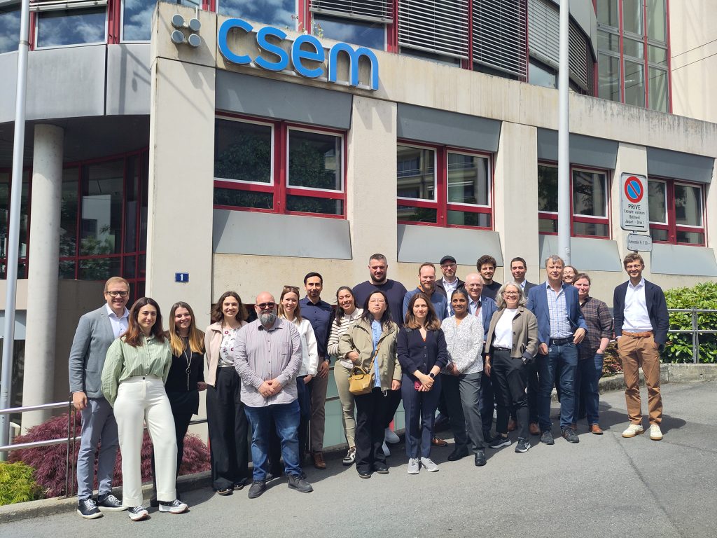
The four-year WISER project (Waste-derived Innovative Solutions for the Secured and Sustainable Supply of Semiconductor Raw Materials to Europe) officially launched on 1 May 2026. Funded by the European Union under Horizon Europe with nearly €8 million, the project brings together 13 organisations from across Europe (CSEM, Kore Metals, Université de Sherbrooke, COMET, NTNU, Recma, Topsil GlobalWafers, IKZ Berlin, PowerShift, AMIRES, NTUA and Advanced Isotopic Analysis) to develop and demonstrate innovative technologies for recovering antimony, silicon and silver, three materials essential to Europe’s semiconductor and clean technology industries.
The consortium spans the full semiconductor value chain, from raw material recovery and purification to wafer manufacturing, qualification and traceability. Through this collaborative approach, WISER aims to create a pathway towards a more sustainable, competitive and resilient European semiconductor ecosystem.